Why it matters: AMD may not manufacture its own chips anymore, but that hasn't stopped it from investing in research and custom process technologies for its chips. Now, the company has its sights on the innovative material that's set to replace organic substrates and revolutionize chip packaging – glass. A new patent covers the use of glass core substrates, possibly for advanced multi-chiplet processors.
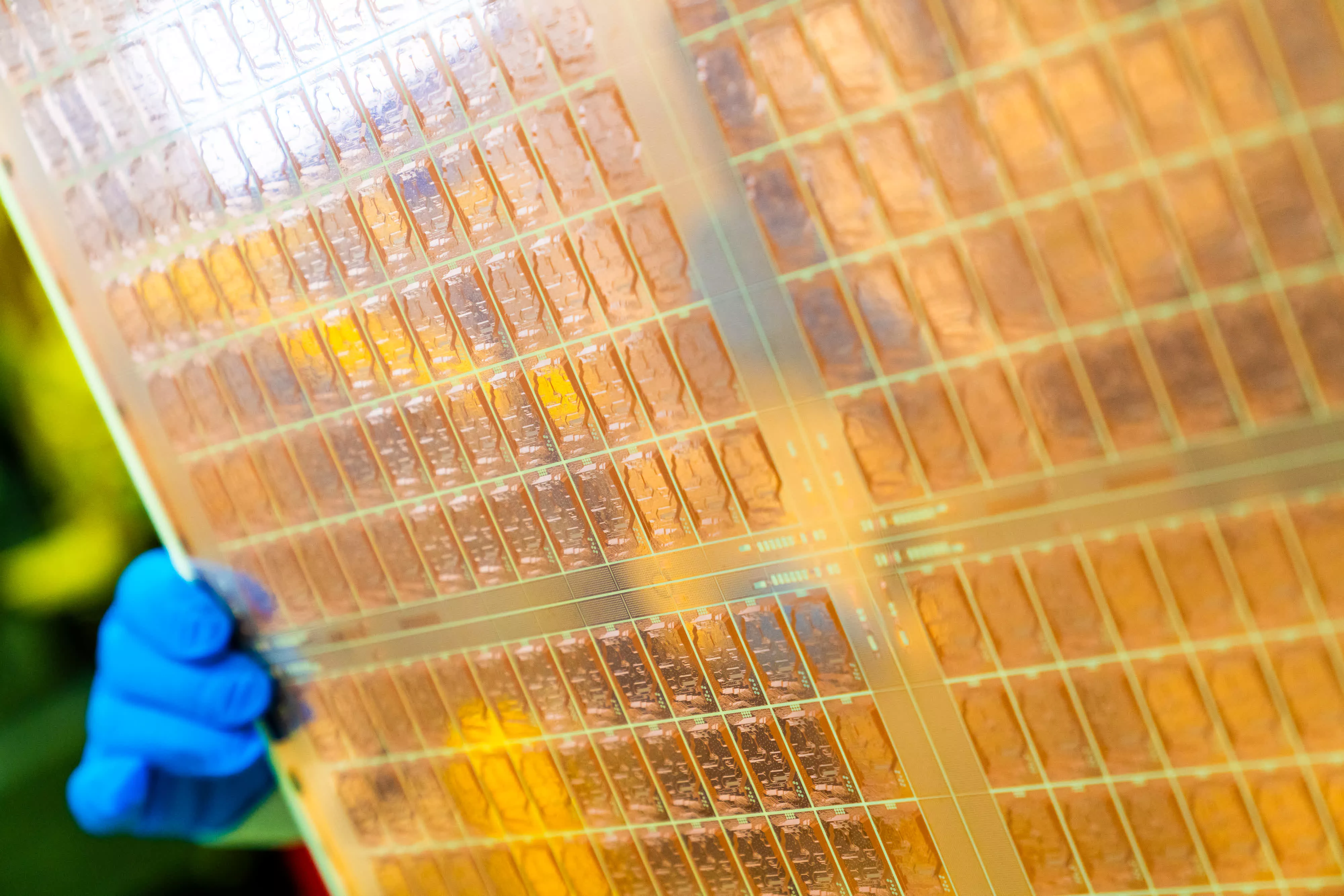
Glass substrates are ultra-thin, flat, transparent sheets made of high-purity silica or borosilicate glass. They serve as a base for semiconductor devices, enabling advanced packaging and interconnect solutions. Compared to silicon or organic substrates, glass offers superior thermal stability, reduced signal loss, and exceptional dimensional accuracy, making it ideal for high-frequency applications like 5G and AI processing.
However, integrating glass substrates into chip designs is not without its challenges. One of the key hurdles, as outlined in AMD's patent and summarized by Tom's Hardware, is the implementation of Through Glass Vias (TGVs) – vertical pathways within the glass core that transmit data signals and power. While techniques like laser drilling, wet etching, and magnetic self-assembly are being explored, the latter two remain relatively novel technologies in this domain.

Another crucial component addressed in the patent is the redistribution layers, which route signals and power between the chip and external components using high-density interconnections. Unlike the main glass core substrates, these layers will continue to utilize organic dielectric materials and copper and will be constructed on one side of the glass wafer.
Interestingly, the patent also describes a method for bonding multiple glass substrates using copper instead of traditional solder bumps. This approach not only ensures strong, gap-free connections but also enhances reliability and eliminates the need for underfill materials, making it suitable for stacking multiple substrates.
Beyond glass substrates, another recent patent by AMD showed that the company was planning to adopt a new method of chip stacking where smaller chiplets are partially overlapped with a larger die. These innovations could eventually arrive on its consumer-oriented Zen CPUs. The company is also exploring novel GPU designs that would be split across multiple GPU chiplet sets.
Of course, other players like Samsung and Intel aren't just sitting around; they're also working to shift to glass substrates as quickly as possible.
